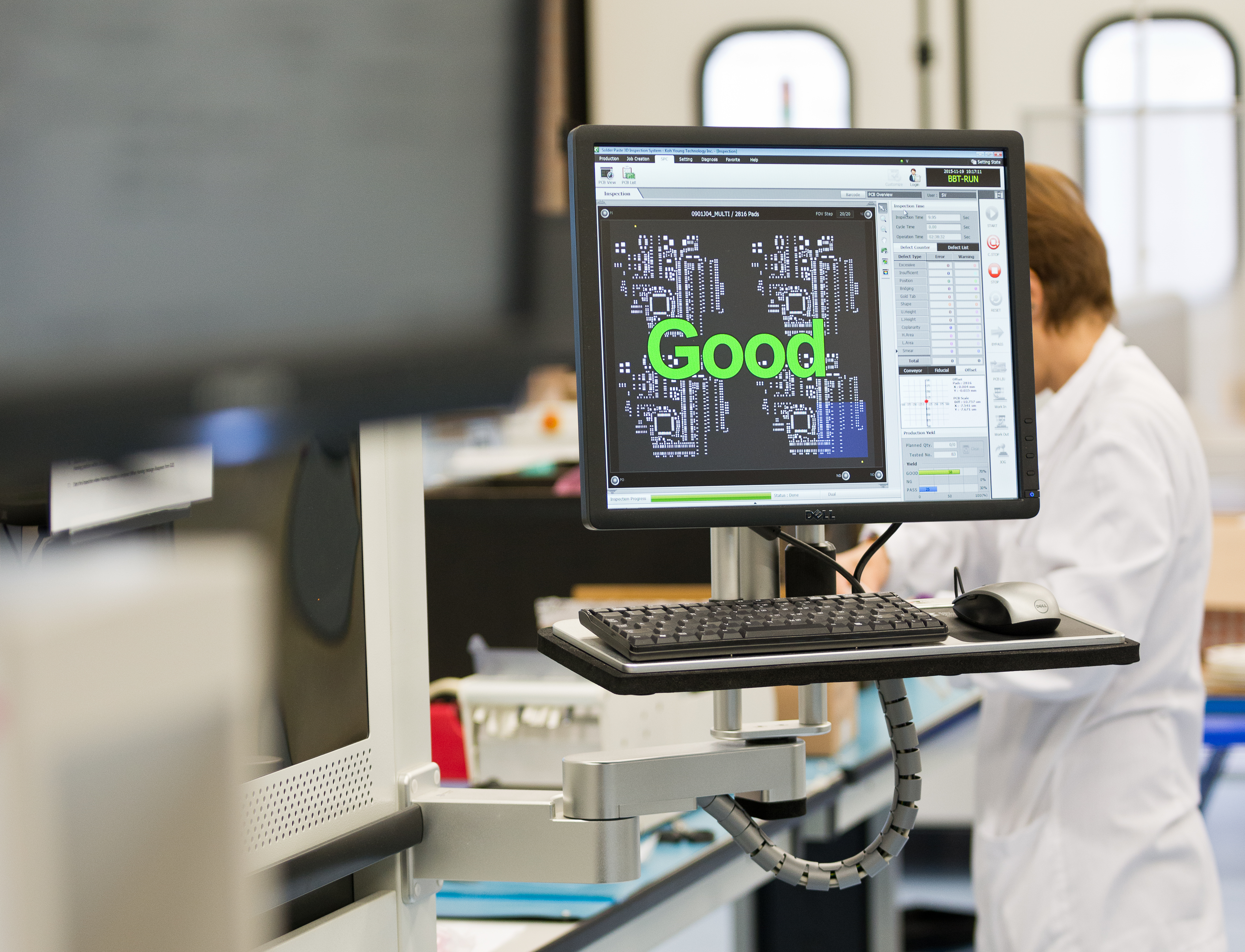
Surface Mount Technology ( S.M.T. ) curiosity
Posted on: Dec. 30, 2022, 1:01 a.m.

Did you know that there is an assembly phase that is little considered but that has a big impact on the S.M.T. assembly process. and it can save you time and money…
what are we talking about?
Let's take a step back; surface mount technology, you can often find it abbreviated with the acronym S.M.T. And it is one of the most used techniques for assembling modern electronic boards. It involves the application of electronic components directly on the surface of the printed circuit, without the need for holes. The products made to use this technique are defined as surface mount devices, acronym SMD.
When we talk about the production process of an electronic board with this technique, it can ideally be summarized in these 4 phases:
1. Procurement of components and materials
2. Solder paste dispensing
3. positioning components on the PCB
4. recast
5. Inspection and testing
One of these stages is often overlooked. . .
We are talking about step number 2! That's right, the dispensing of the solder paste on the PCB is a crucial step thinking in particular of the production of prototypes and therefore the creation of a few specimens with a high level of uncertainty about the result because the greater the probability of design errors.
On the other hand, the prototypes are built in the first instance precisely for the testing and correction of any errors phases and are never in all respects identical to the final product. Many designers have a design plan that involves building multiple prototype phases. . .
What does all this have to do with dispensing solder paste? why does it impact so much in the prototyping phase? . . .keep in mind what you have just read, you will understand shortly.
What is the solder paste dispensing step:
With the surface mount technology, Before positioning the component on the printed circuit, in the appropriate position, it is necessary to deposit a thin layer of solder paste selectively on the pads intended for soldering.
Normally the process takes place by screen printing, i.e. by spatulating (typically with automatic machinery) the solder paste through the openings of a metal stencil adhering to the printed circuit.
The solder paste is made up of a mixture of metal microspheres having a precise statistical distribution of diameters (so-called "type" of the paste), mixed in such proportions as to form - once fused together - a precise alloy.
The set of microspheres is kept together in a pasty form thanks to the surface tension of a liquid called flux, whose function is also to deoxidize the metal surfaces through its own vaporization during the welding process.
If you use the traditional method, you must first make the metal stencil which means having to bear an average cost of around €150 but above all waiting for a time ranging from 3 to 5 working days and which obviously add up to the timing of the entire production process of your tabs.
Today on the creation of prototype boards 4 days are an eternity!!
Let's see some examples of the problems that can be encountered with the traditional method
Imagine you have finished your project, sent the prototypes into production and find out from your supplier, after weeks of waiting, that you have made a mistake on the printed circuit, for example the pads of some QFN components are wrong due to an error on a symbol in the software layouts!
An error on the file is mechanically reflected on the screen printing frame. This translates into more days of waiting to correct the problem, when possible, and in the worst of situations having to redo the stencil for screen printing and then shelling out more money.
Another common situation? . . . You have made your first prototypes, made some corrections with a few modifications to the PCB and you want to produce others to validate what was correct: You are forced to create a new stencil for screen printing.
in addition to this, you have no idea how much solder paste is wasted dispensing a minimum amount of it on a few boards.
Now do you understand why it might be important to have a different method when it comes to producing prototypes?
There is a method that can, in the prototype environment:
- Reduce timing?
- Reduce costs?
- Ensure flexibility?
The answer is obviously YES, YES and YES. . . it's called Jet Printer technology and it's a must of WEP!
Our machines for depositing the solder alloy use the technology called Jet Printer which deposits the solder paste without using the screen printing frames.
In less than a working day, our technicians are able to develop an ad hoc screen printing program for your boards, screen print them and be able to move on to the next phase of positioning the SMD components.
Now think about what happens in the situations seen above as examples. All you have to do is send the corrected file and we will make the few changes to the program and the potentially disastrous situation before will no longer be a problem.
It may seem like a trivial phase and often never considered but as you could well understand it has a big impact on the final result.